Menu
latest blog
Lorem ipsum dolor sit amet, consectetur adipiscing elit. Ut elit tellus, luctus nec ullamcorper mattis, pulvinar dapibus leo.

Types of PCB Copper Foil: Engineer’s Guide to Signal Integrity & Power
In the intricate world of Printed Circuit Board (PCB) manufacturing, the spotlight often falls on the dielectric material—the FR-4, the Polyimide, or the High-Frequency resin. However, the conductor that carries the actual electrical signal is often treated as a commodity. This is a critical mistake in modern electronics design.
Copper foil is the “vascular system” of the PCB. As we push the boundaries of technology with 5G/6G telecommunications, AI-driven data centers, and high-voltage Electric Vehicles (EVs), the generic “1 oz copper” specification is no longer sufficient. The grain structure, surface roughness, and tensile strength of the copper foil embedded in the Copper Clad Laminate (CCL) dictate the board’s performance.
At Credisyn, we do not just laminate copper to resin; we engineer the interface. Understanding the different types of copper foil is essential for PCB designers, signal integrity engineers, and procurement managers aiming to optimize performance and yield.
This comprehensive guide explores the metallurgy, manufacturing processes, and selection strategies for PCB copper foils, detailing how Credisyn integrates these materials to build world-class laminates.
1. The Fundamental Divide: Manufacturing Methods
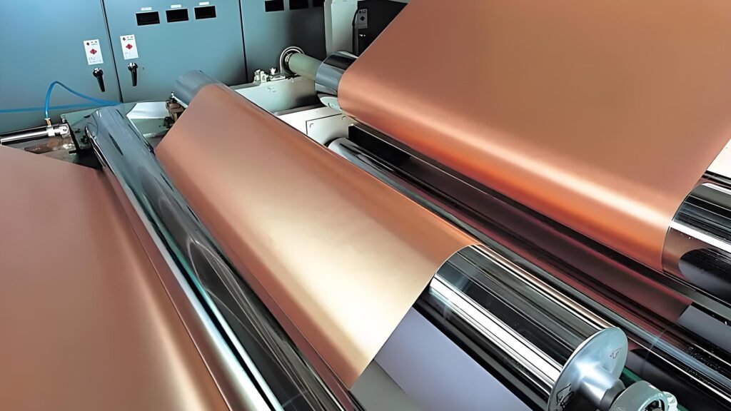
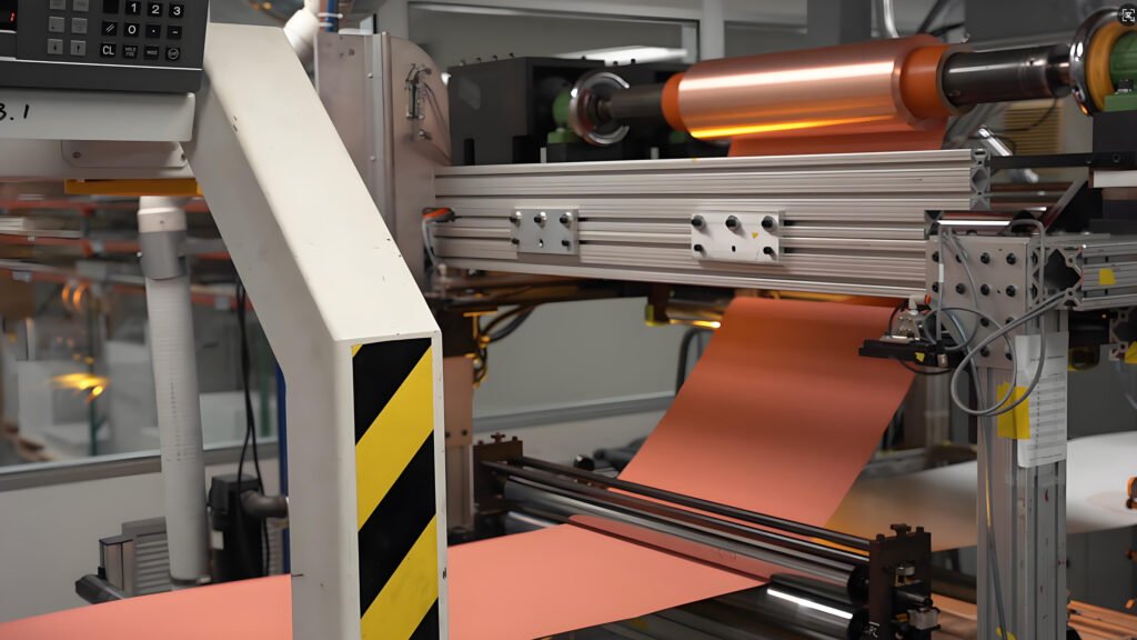
All copper foil starts as pure copper cathode, but how it is formed into a thin sheet defines its mechanical and electrical destiny. There are two primary manufacturing methods used in Credisyn’s CCL production: Electro-Deposited (ED) and Rolled Annealed (RA).
A. Electro-Deposited (ED) Copper Foil
The Industry Workhorse ED copper accounts for the vast majority of rigid PCB applications, from standard consumer electronics to complex multilayer servers.
1. The Manufacturing Process
ED foil is created through electrolysis.
- Dissolution: High-purity copper shot is dissolved in a sulfuric acid solution to create a copper electrolyte bath.
- Deposition: A large, slowly rotating titanium drum (the cathode) is partially submerged in this bath. As a high current is applied, copper ions migrate from the solution and plate onto the drum’s surface.
- Stripping: As the drum rotates out of the bath, the thin layer of copper is stripped off, washed, and wound into rolls.
2. Grain Structure and Characteristics
The electrolysis process creates a vertical, columnar grain structure.
- Vertical Grain: Think of a dense forest of trees standing side-by-side. This structure provides excellent vertical conductivity and good etching characteristics.
- Surface Difference: The side touching the smooth titanium drum becomes the “Shiny Side” (Drum Side). The side facing the electrolyte solution grows rougher as crystals build up; this is the “Matte Side.”
- Credisyn Application: We utilize high-grade ED copper for our CS-FR-170 (High-Tg) and CS-HighSpeed series. The matte side provides the necessary “tooth” or roughness to mechanically lock into the epoxy resin during the lamination process.
3. Pros and Cons
- Pros: Cost-effective, wide range of thicknesses (from 5μm to 400μm+), excellent etchability for fine lines.
- Cons: Lower ductility (flexibility). Under repeated bending, the vertical grain structure can fracture (work hardening).
B. Rolled Annealed (RA) Copper Foil
The Specialist for Flexibility RA copper is the standard for Flexible Printed Circuits (FPC) and rigid-flex applications where dynamic bending is required.
1. The Manufacturing Process
RA foil is made mechanically, not chemically.
- Ingot Casting: It starts as a solid copper ingot.
- Rolling: The ingot is passed through a series of heavy steel rollers, compressing it thinner and thinner, much like rolling out dough.
- Annealing: The heat generated (or applied) during rolling re-aligns the grain structure.
2. Grain Structure and Characteristics
The rolling process creates a horizontal, laminar grain structure.
- Horizontal Grain: Think of a stack of paper sheets. When you bend a stack of paper, the sheets slide over each other. This structure allows RA copper to withstand repeated flexing without cracking.
- Smoothness: Both sides of RA copper are naturally very smooth, which is excellent for signal integrity but challenging for resin adhesion (requiring specialized chemical treatments).
3. Pros and Cons
- Pros: Superior ductility and elongation. Ideal for dynamic flex applications (e.g., disk drive hinges, folding smartphones). Very smooth surface (Low profile).
- Cons: Higher cost than ED. Limited width availability. Harder to etch very fine lines due to the horizontal grain density.
2. Surface Roughness: The Critical Parameter for Signal Integrity
In the past, “rougher was better.” A rough copper surface acted like an anchor, digging into the resin to ensure high peel strength. However, in the age of High-Frequency electronics (5G, Radar, PCIe Gen 5), roughness is the enemy.
This is due to the Skin Effect.
Understanding the Skin Effect
As frequency increases, alternating current (AC) is forced to flow along the outer edges (the “skin”) of the conductor rather than through the center.
- At 50Hz (Grid Power): Current uses the whole wire.
- At 10GHz (5G/Radar): The “Skin Depth” is less than 0.7 microns.
If the copper surface is rough (full of microscopic peaks and valleys), the high-frequency signal must travel up and down every mountain and valley. This increases the path length, leading to:
- Insertion Loss: The signal gets weaker.
- Phase Delay: The signal arrives late.
Credisyn’s Foil Classifications by Profile
To balance adhesion (needs rough) with signal integrity (needs smooth), Credisyn selects specific foil profiles for different CCL product lines.
1. Standard ED (STD)
- Roughness (Rz): 5.0μm – 10.0μm.
- Application: Standard FR-4, LED lighting, Consumer electronics.
- Pros: Excellent peel strength (>1.4 N/mm). No risk of delamination.
- Cons: High signal loss above 1GHz.
2. Low Profile (LP)
- Roughness (Rz): < 5.0μm.
- Application: Mid-range servers, Industrial controls.
- Credisyn Use: Used in our Mid-Loss materials to bridge the gap between cost and performance.
3. Very Low Profile (VLP)
- Roughness (Rz): < 3.0μm.
- Application: High-speed digital boards, RF modules.
- Tech: Manufacturers use additives in the electrolyte bath to limit crystal growth height, keeping the matte side smoother.
4. Hyper Very Low Profile (HVLP)
- Roughness (Rz): < 1.5μm (almost mirror-like).
- Application: Credisyn’s 5G & AI Series. Used for 77GHz automotive radar and 112Gbps data links.
- Challenge: How do you stick mirror-smooth copper to resin?
- Credisyn Solution: We use advanced chemical bonding treatments (Silane coupling agents) on the copper surface, rather than relying solely on mechanical locking. This allows us to achieve Peel Strength > 0.8 N/mm even with ultra-smooth foil.
3. Specialized Foil Types: Beyond Standard
Credisyn creates tailored solutions for specific industry challenges. Here are the specialized foil types integrated into our high-performance laminates.
A. Reverse Treated Foil (RTF)
The “Best of Both Worlds” for Multilayer Boards.
In standard ED copper, the “Matte Side” (rough) is bonded to the prepreg, and the “Shiny Side” (smooth) is on top for etching.
- The Issue: For fine-line etching (<3 mil trace width), a rough surface makes it hard to etch clean, straight lines. You want the top surface to be rough for photoresist adhesion, but the bottom (bonded) side to be smooth for signal.
- The RTF Solution: The manufacturer treats the drum side (shiny side) to create a micro-roughness for bonding to the resin. The matte side is then used as the outer surface.
- Benefit: The low profile of the drum side faces the resin (good for signal integrity), while the matte side faces out (good for photoresist adhesion).
- Credisyn Insight: RTF is the standard for our HDI (High Density Interconnect) laminates, allowing for finer circuit geometries without sacrificing bond strength.
B. Heavy Copper Foil
The Powerhouse for EVs and Renewables.
While standard PCBs use 0.5oz (18μm) or 1oz (35μm) copper, Power Electronics require mass.
- Specs: 3oz (105μm) to 12oz (420μm) and beyond.
- Application: Planar transformers, EV Battery Management Systems (BMS), Solar Inverters.
- Manufacturing Challenge: Thick copper is hard to laminate without creating voids (air bubbles) at the edge of the copper tracks.
- Credisyn Solution: For our CS-Heavy-600 series, we use Heavy Copper foil with a specialized “High-Flow” prepreg. The resin rheology is adjusted to flow deep into the spaces between thick copper tracks, ensuring zero voids and high voltage isolation.
C. Double-Treated Foil (DTF)
The Efficiency Booster.
Usually, a PCB fabricator must mechanically scrub or chemically micro-etch the outer copper surface before applying photoresist to ensure it sticks.
- The Foil: DTF is treated on both sides by the foil manufacturer.
- Benefit: It eliminates the cleaning/scrubbing step at the PCB factory, reducing water usage and process time.
- Drawback: It is sensitive to handling. Scratches cannot be “scrubbed out.”
D. Battery Grade Copper Foil
The Lithium-Ion Backbone.
While not for the PCB itself, Credisyn’s foil division produces copper for Li-Ion battery anodes.
- Requirement: Ultra-high tensile strength and elongation to survive the expansion/contraction of battery charging cycles.
- Thickness: Extremely thin (6μm – 8μm) to maximize energy density.
4. Technical Specifications: Reading the Datasheet
When you review a Credisyn Technical Datasheet (TDS) or an IPC-4101 slash sheet, you will encounter specific metrics regarding the copper. Here is how to interpret them.
1. Peel Strength (IPC-TM-650 2.4.8)
- Definition: The force required to peel a 1-inch wide strip of copper off the laminate.
- Unit: N/mm or lb/in.
- Standard: > 1.05 N/mm for standard 1oz copper.
- Relevance: Critical for thermal shock reliability. If peel strength is low, pads will lift off the board during soldering rework or component replacement.
- Credisyn Standard: We maintain a CPK > 1.33 for peel strength, ensuring robust adhesion even after multiple reflow cycles.
2. Elongation (IPC-TM-650 2.4.18)
- Definition: How much the copper can stretch before it snaps.
- Classification:
- Class 1 (Standard): > 5% elongation.
- Class 3 (High Temperature): > 10% elongation.
- Relevance: High elongation (High Ductility) is vital for multilayer boards. As the board heats up, the Z-axis expands. If the copper in the plated through-holes (PTH) cannot stretch, it will crack (Barrel Crack), causing an open circuit.
- Credisyn Tech: We use HTE (High Temperature Elongation) ED copper for all multilayer laminates to prevent barrel cracks.
3. Tensile Strength
- Definition: The maximum stress the copper can withstand while being stretched.
- Relevance: Important for handling thin cores (inner layers) during manufacturing to prevent tearing.
5. The Treatment Layer: The Invisible Hero
Copper oxidizes. If you leave bare copper in air, it turns green (verdigris). To prevent this and ensure adhesion, raw copper foil goes through a complex “Passivation” and “Treatment” line before it reaches Credisyn’s lamination press.
The Treatment involves three stages:
- Bonding Stage: Nodules of copper/copper-oxide are plated onto the matte side to increase surface area (the “teeth”).
- Thermal Barrier (Brass/Zinc): A microscopic layer of brass or zinc is applied. This prevents the copper atoms from migrating into the epoxy resin during the high-heat lamination.
- Why it matters: Copper accelerates the decomposition of epoxy. Without this barrier, the resin touching the copper would become brittle and degrade.
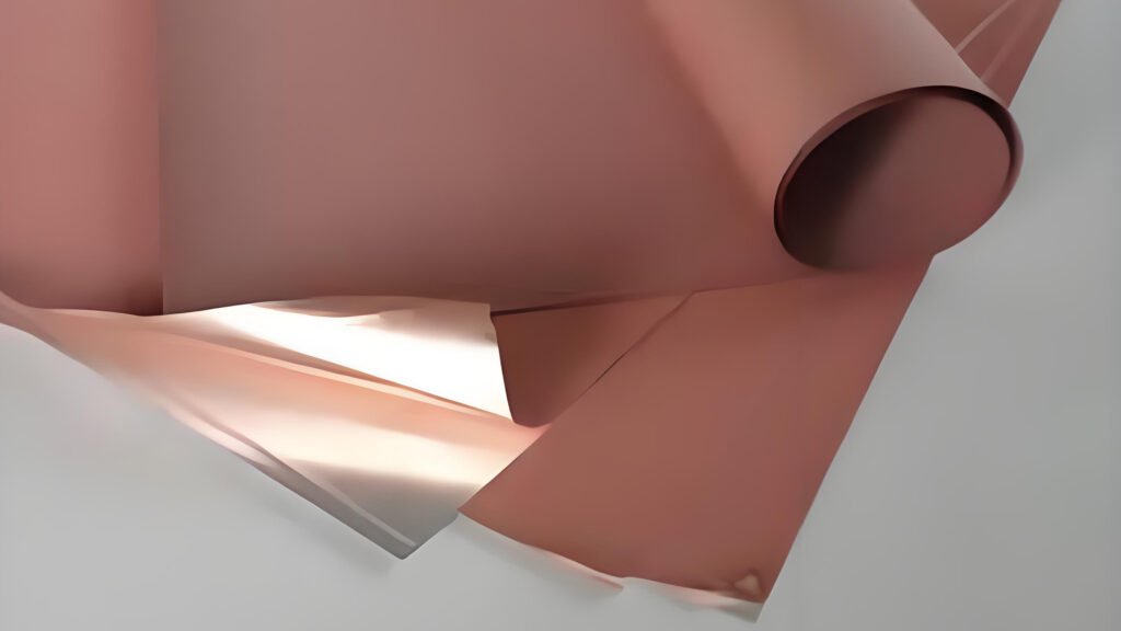
- Anti-Tarnish/Passivation (Chromate): A final layer (usually Chrome-based, though Credisyn offers Chrome-Free options) is applied to prevent oxidation during storage. This gives the copper its characteristic pinkish-orange color.
Credisyn Quality Note: We use AOI (Automated Optical Inspection) on incoming copper rolls to detect “pinholes” in this treatment layer. A pinhole in the barrier can lead to localized resin degradation or “measling” spots.
6. Credisyn’s Selection Guide: Matching Foil to Application
Choosing the right copper is a collaborative process between the designer and the material supplier. Here is Credisyn’s quick guide to selection:
Scenario A: The 5G Base Station Antenna
- Requirement: Low Signal Loss at 28GHz, consistent Impedance.
- Credisyn Recommendation: HVLP Copper (Rz < 1.5μm) combined with CS-HighSpeed (Low Dk/Df) resin.
- Why: Minimizes skin effect losses. The smooth surface ensures the effective dielectric constant doesn’t shift.
Scenario B: The Automotive EV Charger (OBC)
- Requirement: 400V operation, high heat dissipation, vibration resistance.
- Credisyn Recommendation: Heavy Copper (3oz – 6oz) with HTE (High Temp Elongation) properties.
- Why: Heavy copper handles the current; HTE properties survive the thermal cycling of the vehicle engine bay (-40°C to +125°C).
Scenario C: The Smartphone Camera Module (Rigid-Flex)
- Requirement: Folded installation, extremely fine lines.
- Credisyn Recommendation: RA (Rolled Annealed) Copper.
- Why: Prevents cracking during the folding installation process.
Scenario D: The General Industrial Controller
- Requirement: Cost-efficiency, durability.
- Credisyn Recommendation: Standard ED Copper (Class 3 Elongation).
- Why: Provides the best balance of cost, etch speed, and reliable adhesion.
7. Quality Control and Storage: The Credisyn Difference
Copper foil is perishable. Its shelf life is determined by the quality of the anti-tarnish coating and the storage environment.
Storage Protocols
At Credisyn, copper foil inventory is managed in a strict Class 1000 cleanroom environment with controlled humidity (< 50% RH) and temperature (20-25°C).
- Oxidation Risk: If humidity spikes, the edges of the roll can oxidize. This leads to “Edge Delamination” in the final PCB.
- Vacuum Sealing: All our prepregs and copper foils are vacuum-sealed until the moment of layup.
Defect Prevention
We monitor for specific copper defects:
- Pits and Dents: Can cause open circuits in fine-line traces.
- Wrinkles: Caused by uneven tension during rolling; leads to lamination voids.
- Resin Spots: Contamination on the foil prevents etching, causing short circuits.
Our Traceability System (QR Code) allows us to trace every sheet of laminate back to the specific master roll of copper foil and the specific bath parameters used by our supplier, ensuring total accountability for automotive clients (IATF 16949 compliant).
Conclusion: The Copper Foundation
Copper foil is more than just a metal sheet; it is a sophisticated component engineered for specific physical and electrical behaviors. Whether you are battling the Skin Effect in a 5G server or managing thermal loads in an EV inverter, the type of copper you choose determines the ceiling of your product’s performance.
At Credisyn, we understand these nuances. By partnering with top-tier foil foundries and applying our proprietary lamination techniques, we deliver Copper Clad Laminates that maximize the potential of every micron of copper.
Don’t let standard copper limit your advanced designs. Explore Credisyn’s range of High-Speed, High-Power, and Automotive-Grade laminates today. Contact our technical team to discuss which copper profile—HVLP, HTE, or Heavy Cu—is right for your next innovation.
FAQ: Copper Foil Basics
Q: What is the difference between “1 oz” and “2 oz” copper? A: “1 oz” refers to the weight of copper per square foot. It translates to thickness: 1 oz ≈ 35μm (1.37 mils), 2 oz ≈ 70μm. Heavier copper carries more current.
Q: Can I use RA copper for rigid boards? A: Yes, especially for high-frequency applications due to its smoothness, but it is more expensive than ED copper and harder to source in wide panels.
Q: Why does my copper look pink vs. red? A: This depends on the anti-tarnish treatment (brass, zinc, or chromate). The color does not indicate the purity of the copper (which is always >99.8%) but rather the passivation layer used.
Q: Does Credisyn manufacture the copper foil itself? A: Credisyn manufactures the Copper Clad Laminate. We source raw foil from strategic partners who adhere to our strict metallurgical specifications, then we perform the lamination, curing, and quality assurance processes.
Paper core copper-clad substrate
Glass cloth copper-clad substrate
Cloth paper composite copper-clad substrate
Cloth felt composite copper-clad substrate
Paper core copper-clad substrate
Glass cloth copper-clad substrate
Cloth paper composite copper-clad substrate
Cloth felt composite copper-clad substrate
Credisyn quality copper clad laminates for global electronics
Credisyn-Professional CCL manufacturer, delivering reliable electronic substrate solutions worldwide.
Quick Link
Email: info@credisyn.com
Quick Link
Add: No. 18 Hong Kong Middle Road, Qingdao, China
Copyright © 2025 Website Title Copper Cladd Laminated Supported by Credisyn technology